Difference between revisions of "Project/VHDL"
m (→Components) |
|||
| (3 intermediate revisions by the same user not shown) | |||
| Line 159: | Line 159: | ||
We start the architecture with our component instantiation. We can "map" the signals and generics inside our component to internal or external signals in our PWM output entity, and fixed values like the binary '0' for our reset signal. We do not want our counter to reset to its 0-state. Instead, the counter will wrap around if we count further than the bit capability. This will represent the PWM cycle in our design. If the current counter value is lower than the desired one in the <code>pwm_value</code> input, the output of our design will be high. Otherwise, the output will be low. For our 8 bit (0 to 255 value) PWM design, a PWM value of 63 will mean a quarter of the period time high, and three quarters of the period time low output value. | We start the architecture with our component instantiation. We can "map" the signals and generics inside our component to internal or external signals in our PWM output entity, and fixed values like the binary '0' for our reset signal. We do not want our counter to reset to its 0-state. Instead, the counter will wrap around if we count further than the bit capability. This will represent the PWM cycle in our design. If the current counter value is lower than the desired one in the <code>pwm_value</code> input, the output of our design will be high. Otherwise, the output will be low. For our 8 bit (0 to 255 value) PWM design, a PWM value of 63 will mean a quarter of the period time high, and three quarters of the period time low output value. | ||
[[File:pwm_output.png]] | |||
This is a representation of the PWM output design in an actual device. 196 is the input of our PWM value. All bits of count_internal are shown, and indeed forms a counter that counts upwards. It's shown as a line representing the value of count_internal, clearly a sawtooth pattern. At the bottom is our PWM output. It's most of the time high, and also a small part low. For 196 of the 255 parts, it's high, and the rest low signal level. | |||
The way this actually works is as follows: The compiler program implements, besides our own PWM design, also the design of a logic analyzer. The data from this is sent over the programming port to the computer. The signals on our picture actually represents the signals inside our device. This is a very helpful tool to debug our designs. The FPGA in this case is running at full speed, with real-life signals, while we can monitor all the signal levels we want inside. In Altera terms, this is called a "Signal Tap". The data collected from our selected lines is stored in the device's internal memory blocks and sent over the JTAG programming port. | |||
== Shifting <s>reality</s> registers == | |||
Let's take a look at the usability of our PWM design. A single output, but besides from a clock input, we spent 8 inputs on defining a PWM value for our design. If we have multiple PWM designs in an FPGA, or other needs for inputting data, we can very easily surpass the device's pin count. Fortunately, an easy to implement communication protocol exists for inputting data in a serial fashion: the SPI or Serial Peripheral Interconnect bus. The SPI bus consists of a small number of pins: a data pin, clock pin and a latch pin. Communication runs from a master device who generates the clock and latch signals, and a slave device who reacts to these master signals. Data direction can be either or both ways. To be able to communication to multiple slave devices, SPI bus masters can implement a Slave Select pin for each slave, or slave devices can pass through data to another slave (also known as daisy-chaining). | |||
[[File:daisy_chain.png]] | |||
We are going to use this SPI bus protocol to provide the 8 bits needed for our PWM design. | |||
<pre> | |||
library ieee; | |||
use ieee.std_logic_1164.all; | |||
use ieee.std_logic_unsigned.all; | |||
entity spi_pwm is | |||
port( | |||
clock : in std_logic; | |||
pwm_out : out std_logic; | |||
spi_data : in std_logic; | |||
spi_clock : in std_logic; | |||
spi_latch : in std_logic | |||
); | |||
end entity spi_pwm; | |||
architecture behavioural of spi_pwm is | |||
signal spi_data_latch : std_logic_vector(7 downto 0); | |||
signal spi_latch_shift : std_logic_vector(1 downto 0); | |||
signal spi_data_register : std_logic_vector(7 downto 0); | |||
component pwm_output is | |||
port( | |||
pwm_clock : in std_logic; | |||
pwm_value : in std_logic_vector(7 downto 0); | |||
pwm_out : out std_logic | |||
); | |||
end component pwm_output; | |||
begin | |||
spi_shift : process (spi_clock) | |||
begin | |||
if spi_clock'event and spi_clock = '1' then | |||
spi_latch_shift <= spi_latch_shift(0) & spi_latch; | |||
spi_data_register <= spi_data_register(6 downto 0) & spi_data; | |||
if spi_latch_shift = "01" then | |||
spi_data_latch <= spi_data_register; | |||
end if; | |||
end if; | |||
end process spi_shift; | |||
pwm_process : pwm_output | |||
port map( | |||
pwm_clock => clock, | |||
pwm_value => spi_data_latch, | |||
pwm_out => pwm_out | |||
); | |||
end behavioural; | |||
</pre> | |||
Let's take a closer look at <code>spi_latch_shift <= spi_latch_shift(0) & spi_latch;</code>. When a rising edge of spi_clock occurs (from the process declaration), the new value for <code>spi_latch_shift</code> will be: <code>spi_latch_shift(0)</code> and <code>spi_latch</code>. <code>spi_latch_shift</code> is defined as <code>spi_latch_shift(1 downto 0)</code> so the data in <code>spi_latch_shift(0)</code> will become <code>spi_latch_shift(1)</code>. What happens with the old value of <code>spi_latch_shift(1)</code>? it's lost!. We effectively created a history buffer for <code>spi_latch</code>. We know the current value, because it's assigned to <code>spi_latch_shift(0)</code>, and we know what it was a clock cycle before that, in <code>spi_latch_shift(1)</code>. This enables us to see if the latch signal has changed in value. In <code>if spi_latch_shift = "01" then</code> we test if the value has changed from '0' to '1', and if that is the case, we latch the data in <code>spi_data_register</code> into <code>spi_data_latch</code>. <code>spi_data_latch</code> is also a shift register for <code>spi_data</code>, but it is 8 bits wide. We know what the value for <code>spi_data</code> was for 8 clock cycles before, and we use these to fill our <code>spi_data_latch</code>, and ultimately our value for <code>pwm_value</code>. | |||
[[Category: Project]] | [[Category: Project]] | ||
Latest revision as of 14:41, 1 January 2016
Introduction
Ever wished you could make your own integrated circuits? Is regular logic just not doing the trick for you? This project is all about programmable logic, and how you can define your own digital circuits yourself. Welcome to the wonderful world of CPLD's and FPGA's!
History
There was a time that, if you wanted a new logic function on your custom PCB, you had to have more chips. TTL logic chips that is. With quad NAND gates like the 74HC00, and a whole range of different logic functions, PCB's often became very complex. Often, not all the gates of such integrated circuits were used. Late 1970's, one of the first well-known programmable logic devices hit the streets. The Programmable Array Logic or PAL chips were made by Signetics, and at a later stadium copied by National Semiconductor, Texas Instruments and AMD. With names as "PAL16L8" and "PAL22V10", you could define your own logic in a One Time Programmable chip. It worked with fuses and could be programmed only once. It was very convenient to define your own logic gates, without the need for all those specific logic chips. At a later stadium, Electrically erasable GAL devices were pin-to-pin compatible and the road was set for devices that implemented large quantities of logic gates in a single device.
The PAL and GAL devices had a very limited amount of pins, and Complex Programmable Logic Devices or CPLD's were a great improvement on both pin count and complexity. But it wasn't until the Field Programmable Gate Arrays or FPGA's when the functionality and usability really took off. Of course, all of these devices had to be programmed in a certain way, and most of the time it means really defining what gate and functions had to active. There was a great need for a programming language to define the functionality of digital circuits. The Hardware Description Language or HDL was on its way!
Different flavors
The current market for programmable logic is roughly separated in a few brands:
- Xilinx, the largest manufacturer. Popular chips include the Spartan series, Virtex and Zynq devices.
- Altera (now owned by Intel). Inventors of the MAX CPLD's, Cyclone FPGA's and Stratix series.
- Actel. A smaller brand, but still the Igloo and ProAsic series are pretty well known.
- Lattice has the iCE series, MachXO and ispMACH devices.
There are a number of other smaller manufacturers, but these are the most well known ones. But if you want to program a CPLD or FPGA, you have several options. Most software packages offer the use of schematic diagrams to define the functionality inside, but while your designs get more complex, you will want to learn a HDL or Hardware Description Language. Two are commonly known:
- VHDL or VHSIC Hardware Description Language. This is most commonly used in Europe.
- Verilog is more used in the USA.
Building blocks
A modern FPGA device can hold several items to implement your design:
- Logic Elements or Cells. This is the most basic building block and it is used to implement all of your digital functions.
- Memory. These can help to store larger amounts of data in ROM, RAM, Dual port RAM and large buffers such as a First-In, First-Out (FIFO) buffers or shift registers.
- Multipliers. These help a great deal in signal processing and are therefore also referred as DSP blocks.
- Transceivers. Many well-equipped FPGA's offer very fast serial communication blocks. Almost all modern digital communication protocol implement these: HDMI, USB3.x, SDI, SATA and SAS, PCI express and many others.
- SOC's. Some FPGA's are accompanied by microprocessor blocks. Examples include a ZynQ, Cyclone V and SmartFusion devices.
When you are defining your functions in VHDL, you are using the LE's or Cells inside your FPGA. If you want to use other, device-specific blocks, this can be done in two ways. In the first way a specific specialized block is inferred. Through your definition of a function, the computer who reads your VHDL decides that it can best be implemented with a specialized block. Define a 1024-position buffer, and your compiler shortly decide it can best be implemented with a memory block. The other way is by instantiation: You specifically tell that you want to use a DSP, or transceiver block. You will have to define what settings need to be applied, and what configuration you need. This has also a disadvantage: If you want to use a different device, it might not recognize these instantiations!
VHDL first steps
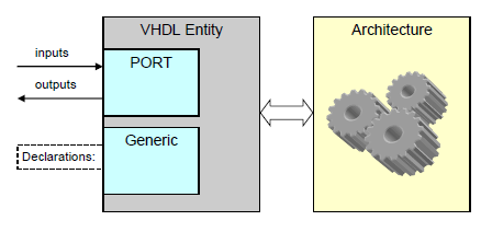
So lets start with VHDL and defining our very first functionality. First, you will have to know something about the language. Every VHDL design has at least one entity. An entity can best be described as a black box. This black box can have one or more ports. Input ports, output ports, or even bidirectional ports. Also, an entity can have generic declarations. You can use this to make your design flexible. For example, you can define a counter function, with a clock and reset input, and a count output port. It can be an eight bit counter, or 16, or 22, or 47.. You could define the amount of bits in a generic declaration.
Once we have our entity, with all ins and outs, we need to define what's inside our black box! In the example of the counter, we can have a regular binary counter, or one with decoded outputs. Or maybe an alternative way of counting? The functionality inside our black box is defined in the architecture.
library ieee;
use ieee.std_logic_1164.all;
use ieee.std_logic_unsigned.all;

entity binary_counter is
 generic(
  counter_width : natural := 8 -- we want an 8 bit counter by default.
 );
 port(
  clock : in std_logic;
  reset : in std_logic := '0';

  count : out std_logic_vector(counter_width-1 downto 0)
 );
end entity binary_counter;

architecture behavioural of binary_counter is

 signal count_internal : std_logic_vector(counter_width-1 downto 0);

begin

 counter : process (clock)
 begin
  if clock'event and clock = '1' then -- this means the rising edge of signal "clock"
   if reset = '1' then
    count_internal <= (others => '0'); -- this means all lines are defined to '0'
   else
    count_internal <= count_internal + 1;
   end if;
  end if;
 end process counter;

 count <= count_internal;

end architecture;
- "Counter, schmounter! I have an Arduino and it can count very well!"
You are very right. A counter can also be implemented in other ways, but programmable logic has several advantages over a microcontroller or microprocessor. These devices work with a defined program, and have a sequential execution of instructions. An FPGA works in a different way. All processes happen in parallel, and every single clock cycle. You can very easily run different processes with totally unrelated clocks and define a way of communicating with each other. You can define all kinds of functions you like inside an FPGA, including one of a microcontroller. This is referred as a "softcore processor". Examples are the Microblaze, NIOS and LEON processor core. An industry standard processor can be defined inside an FPGA, but also, for example, a 19-bit CPU. Possibilities are endless!
So let's take a look how the compiler actually implemented our design!
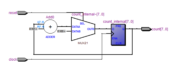
This is somewhat different to what we've expected, but it does the job. The basic functionality of our counter is in the adder, Add0. It adds the binary value 0x01h to the output of a D flipflop register, count_internal[7..0]. The output of the adder can be chosen with a 2-input multiplexer, that also has the binary value of 0x00h as an input. The multiplexer input is set by the reset input. So the output count[7..0] is advanced every clock cycle, unless we assert the reset line. Exactly what we wanted!
There is another thing we can have within the architecture, which can be of good use: A component. A component is an existing entity, which we can use in our current design. Instead of defining every single function again, we can have a hierarchic structure. A lot of simple entity functions can add up to a complex design. Instead of defining a process, we can "port map" a component to existing signals within our design. This is also the way to connect instantiations as well.
Components
Now we've built a very usable counter design in VHDL, let's use this to make a more complex design. A PWM output is a single digital output to represent multiple values. Besides 0% on and 100% on, being a low signal level and a high signal level, we can assign a number of different values to this output. 50% on means that we toggle between low and high in an equally amount of time. 25% means we have 3 times as much low signal level then we have a high signal level. How can we make this in VHDL?
At some point in out design, we have to compare one value to another. The output of this comparison is the output of our PWM design. If we hold the desired PWM value in a register, we have to have a mechanism that steps through all possible values. If we compare these two values, we have built ourselves a PWM output!. The simplest way to step through a range of values is a counter. Let's use our previously built counter for this purpose. To do that, our counter design must be a component of our PWM design. Let's look at the code how this is accomplished.
library ieee;
use ieee.std_logic_1164.all;
use ieee.std_logic_unsigned.all;

entity pwm_output is
 port(
  pwm_clock : in std_logic;
  pwm_value: in std_logic_vector(7 downto 0);

  pwm_out : out std_logic
 );
end entity pwm_output;

architecture behavioural of pwm_output is

 signal counter_value : std_logic_vector(7 downto 0);

 component counter is
  generic(
   counter_width : natural
  );
  port(
   clock : in std_logic;
   reset : in std_logic;
   count : out std_logic_vector(counter_width-1 downto 0)
  );
 end component counter;

begin

 pwm_counter : counter
  generic map(
   counter_width => 8
  )
  port map(
   clock => pwm_clock,
   reset => '0',
   count => counter_value
  );

 pwm_compare : process (pwm_clock)
 begin
  if pwm_clock'event and pwm_clock = '1' then
   if counter_value <= pwm_value then
    pwm_out <= '1';
   else
    pwm_out <= '0';
   end if;
  end if;
 end process pwm_compare;

end behavioural;
In this example, we made an entity, pwm_counter, with some ports. In the architecture of this entity (named behavioural), we defined, apart form a signal, also a component. The name of this component matches our previously made entity counter and the generic and port declaration of this component matches the one of the entity. We now can use this component in our design. One time, but also multiple times, even with a different generic mapping.
We start the architecture with our component instantiation. We can "map" the signals and generics inside our component to internal or external signals in our PWM output entity, and fixed values like the binary '0' for our reset signal. We do not want our counter to reset to its 0-state. Instead, the counter will wrap around if we count further than the bit capability. This will represent the PWM cycle in our design. If the current counter value is lower than the desired one in the pwm_value input, the output of our design will be high. Otherwise, the output will be low. For our 8 bit (0 to 255 value) PWM design, a PWM value of 63 will mean a quarter of the period time high, and three quarters of the period time low output value.
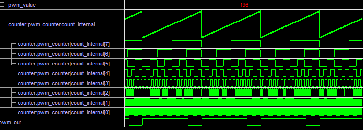
This is a representation of the PWM output design in an actual device. 196 is the input of our PWM value. All bits of count_internal are shown, and indeed forms a counter that counts upwards. It's shown as a line representing the value of count_internal, clearly a sawtooth pattern. At the bottom is our PWM output. It's most of the time high, and also a small part low. For 196 of the 255 parts, it's high, and the rest low signal level.
The way this actually works is as follows: The compiler program implements, besides our own PWM design, also the design of a logic analyzer. The data from this is sent over the programming port to the computer. The signals on our picture actually represents the signals inside our device. This is a very helpful tool to debug our designs. The FPGA in this case is running at full speed, with real-life signals, while we can monitor all the signal levels we want inside. In Altera terms, this is called a "Signal Tap". The data collected from our selected lines is stored in the device's internal memory blocks and sent over the JTAG programming port.
Shifting reality registers
Let's take a look at the usability of our PWM design. A single output, but besides from a clock input, we spent 8 inputs on defining a PWM value for our design. If we have multiple PWM designs in an FPGA, or other needs for inputting data, we can very easily surpass the device's pin count. Fortunately, an easy to implement communication protocol exists for inputting data in a serial fashion: the SPI or Serial Peripheral Interconnect bus. The SPI bus consists of a small number of pins: a data pin, clock pin and a latch pin. Communication runs from a master device who generates the clock and latch signals, and a slave device who reacts to these master signals. Data direction can be either or both ways. To be able to communication to multiple slave devices, SPI bus masters can implement a Slave Select pin for each slave, or slave devices can pass through data to another slave (also known as daisy-chaining).
We are going to use this SPI bus protocol to provide the 8 bits needed for our PWM design.
library ieee;
use ieee.std_logic_1164.all;
use ieee.std_logic_unsigned.all;

entity spi_pwm is
 port(
  clock : in std_logic;
  pwm_out : out std_logic;

  spi_data : in std_logic;
  spi_clock : in std_logic;
  spi_latch : in std_logic
 );
end entity spi_pwm;

architecture behavioural of spi_pwm is

 signal spi_data_latch : std_logic_vector(7 downto 0);
 signal spi_latch_shift : std_logic_vector(1 downto 0);
 signal spi_data_register : std_logic_vector(7 downto 0);

 component pwm_output is
  port(
   pwm_clock : in std_logic;
   pwm_value : in std_logic_vector(7 downto 0);
   pwm_out : out std_logic
  );
 end component pwm_output;

begin

 spi_shift : process (spi_clock)
 begin
  if spi_clock'event and spi_clock = '1' then
   spi_latch_shift <= spi_latch_shift(0) & spi_latch;
   spi_data_register <= spi_data_register(6 downto 0) & spi_data;
   if spi_latch_shift = "01" then
    spi_data_latch <= spi_data_register;
   end if;
  end if;
 end process spi_shift;

 pwm_process : pwm_output
 port map(
  pwm_clock => clock,
  pwm_value => spi_data_latch,
  pwm_out => pwm_out
 );

end behavioural;
Let's take a closer look at spi_latch_shift <= spi_latch_shift(0) & spi_latch;. When a rising edge of spi_clock occurs (from the process declaration), the new value for spi_latch_shift will be: spi_latch_shift(0) and spi_latch. spi_latch_shift is defined as spi_latch_shift(1 downto 0) so the data in spi_latch_shift(0) will become spi_latch_shift(1). What happens with the old value of spi_latch_shift(1)? it's lost!. We effectively created a history buffer for spi_latch. We know the current value, because it's assigned to spi_latch_shift(0), and we know what it was a clock cycle before that, in spi_latch_shift(1). This enables us to see if the latch signal has changed in value. In if spi_latch_shift = "01" then we test if the value has changed from '0' to '1', and if that is the case, we latch the data in spi_data_register into spi_data_latch. spi_data_latch is also a shift register for spi_data, but it is 8 bits wide. We know what the value for spi_data was for 8 clock cycles before, and we use these to fill our spi_data_latch, and ultimately our value for pwm_value.


